WP2 - High efficiency crystalline silicon solar cell technologyTeam leader: Assoc.prof. Mgr. Jakub HolovskĂœ, Ph.D. |
|
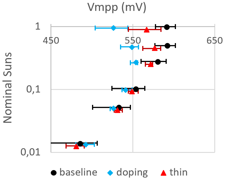
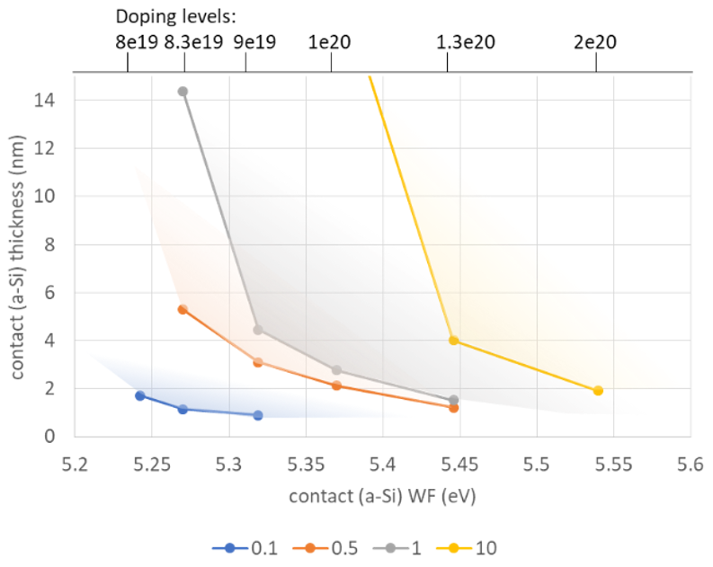
General overviewThe research has one main long-term objective that is 25% efficient solar cell based on silicon passivated contacts technology, optimized for œ sun irradiance and fabricated without use of any kind of chemical vapour or plasma deposition. Only wet chemistry passivation combined with multifunctional transparent oxide layers prepared by Pulsed Laser Deposition or RF Sputtering will be used. The idea of œ sun optimization is supported by many arguments: 1) within the tandem, cells work only below œ sun irradiance, 2) energy cost is high when sunshine is low, 3) capping PV modules to œ of nominal power saves BOS cost and makes system more profitable, 4) reduced current allows for relaxed requirements for contacts. The 25% objective might not be reached by Si cell alone and so tandem with perovskite might be required. For this reason we study hybrid perovskite materials by advanced techniques such as FTPS and in terms of devices we reached 19% efficiency for mixed-halide technology. Fundamentals of solar cell operationThe idea of passivated contacts to silicon were studied experimentally (Fig. 1) and theoretically (Fig. 2) from the point of view of the device performance, mainly under low illumination. In the collaboration with EPFL Neuchatel special samples of silicon heterojunction (SiHJ) solar cells with crystalline silicon/amorphous silicon contact layers. Level of doping and thickness of doped amorphous silicon was varied and the effect on low-light performance was studied and also theoretically simulated, see below. We confirmed experimentally that reducing contact strength does not have effect on voltage at maximum power point Vmpp at low irradiances (Fig. 1). We simulated required parameter windows for of work function (WF) and thickness of contact layer for different thicknesses (Fig. 2). Relaxed requirement for contacts at low level illumination should principally allow more options for contact materials, mainly with less parasitic absorptance (Conrad et al., 2020). In tandem cells we investigated the fundamental role of tunnelling interface and the consequence on shunts (Ventosinos et al., 2018). |
|
|
|
| Fig. 1: Voltage as a function of illumination | Fig. 2: Requirements for given irradiation |
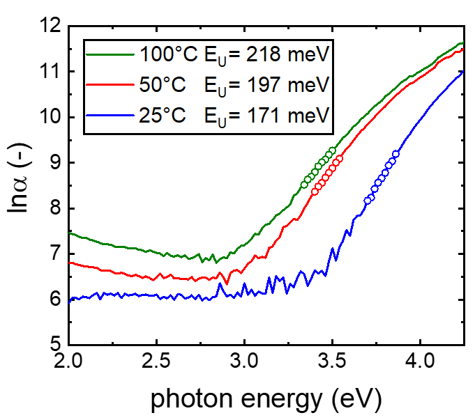
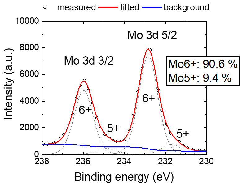
New contact materialsIn the second year of the project we successfully started with our thin-film technology of pulsed laser deposition (PLD). Layer quality was characterized by various methods: photothermal deflection spectroscopy (PDS) was used to determine parasitic absorption and defect density (Fig. 3), X-ray diffraction (XRD) was used for determining crystallinity and X-ray photoelectron spectroscopy (XPS) was used to determine stoichiometry (Fig. 4). We tested effects of deposition temperature and oxygen pressure on layers of MoOX, VOX and WOX (HorynovĂĄ et al., 2020). |
|
|
|
| Fig. 3: MoOX, Abs. coeff., Urbach energy | Fig. 4: MoOX bonding state by XPS |
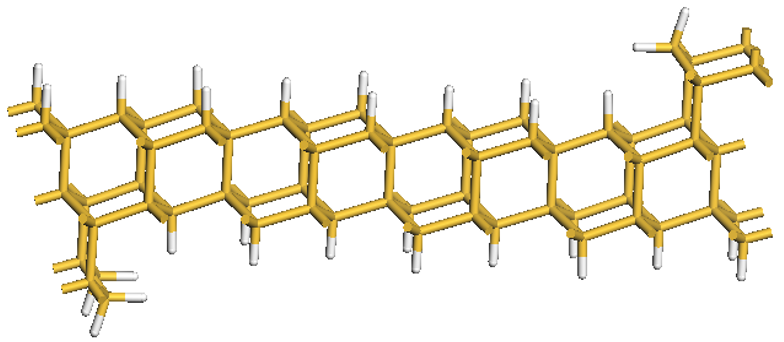
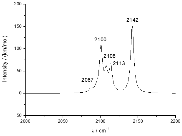
Silicon surfaceHigh efficient contacts require smooth and sharp interfaces with silicon. By tuning pH of silicon etching solution it is possible to induce steps on (111) oriented Si surface facing either â©(11) Ì 2âȘ or â©112 Ì âȘ directions. These are terminated by dihydrides or monohydrides respectively, see Fig. 5. We simulated for the first time vibrational spectra by periodic DFT and we brought new insights into peak assignments, e.g. we confirmed that peak experimentally observed at 2135 cm-1 and simulated at 2142 cm-1 (Fig. 6) is indeed di-hydride under strong stearic interaction and not tri-hydride. Also we explained that satellite peak observed by 0.9 cm-1 above H/Si(111)-(1Ă1) peak at 2083.6 cm-1 is not defect, but an artifact. In parallel to simulations we develop sensitive FTIR techniques (HolovskĂœ et al., 2018). |
|
|
|
| Fig. 5: Si(667) with step facing â©(11) Ì 2âȘ direction | Fig. 6: Vibration spectrum of Si(667)-H |
Hybrid perovskite materials and cellsThe record silicon based technology is now tandem with silicon bottom cell and metal-halide hybrid perovskite top cell with efficiency 28% achieved by Oxford PV. Within this work package our activities are therefore also partially oriented towards thin polycrystalline CH3NH3PbI3 perovskite films and solar cells. In last year, we have achieved significant progress in the solar cell technology, reaching up to 17% conversion efficiencies by new type of TiO2 layer doping (Peter Amalathas et al., 2019) and treatment (Peter Amalathas et al., 2020). Such efficiency is already high enough to allow us performing studies on finished devices that give relevant results, more attractive to photovoltaic community. |
|
|
|
| Fig. 7: perovskite solar cell instability | Fig. 8: instability-related defect absorption |
|
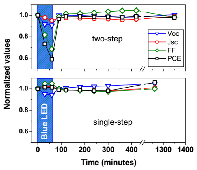
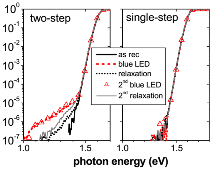
Perovskites devices and also layers exhibit many reversible and irreversible effects. We studied reversible effect of blue illumination on the I-V curves (HolovskĂœ et al., 2019), see Fig 7. Very similar reversible effects were revealed by measurement of sub-bandgap absorption by PDS method and Fourier-transform photocurrent spectroscopy (FTPS) method, see Fig 8. To induce the reversible changes the blue illumination has to be applied from the side of the PbI2-rich side for two step materials. The explanation is the light-induced decomposition of PbI2 into metallic lead and iodine, confirmed by XPS. Because metallic lead is strongly absorbing but does not contribute to photocurrent it can be measured by PDS. On the other hand iodine diffuses and deposit in interstitial positions of CH3NH3PbI3 phase where it creates electronically active deeps states that can be measured by FPTS (HolovskĂœ et al., 2017). One of the explanation of the prominence of the perovskite material is its sharp absorption edge. We study in collaboration with Institute of Physics of ASCR different aspects of absorption edge of novel perovskite materials, e.g. temperature dependence (Ledinsky et al., 2019). |
|
Equipment Pulsed Laser Deposition system (248 nm KrF,150 mJ, 50 Hz, 2 inch substrates, MFC for oxygen, possibility to use hydrogen, with ports fir in-situ ellipsometry, base pressure below 10^-7mbar, substrate heater up to 700 deg C with continuous rotation, 5 target carousel)Spectral Ellipsometer Vollam M2000 (293-1000 nm range, motorized goniometer, motorized X-Y table, options for in-situ)RF sputtering tool (rotational sample holder, heated 600 deg C).Fully robotized wet bench (in the stage of commissioning).Fume hood for only soft chemistry, substrate washing (ultrasonic bath, UV-ozone).Automated I-V setup (KEITHLEY 2401, LED array AAA simulator)Automated EQE (National Instruments DAQ cards and software lock-in analyser, equipped with preamplifiers SR570 and KEITHLEY 428).With the WP3 we share 3-position glove box MBraun filled with nitrogen (equipped with AFM microscope, spin-coater, hot plate and analytical scales). Pulsed Laser Deposition system (248 nm KrF,150 mJ, 50 Hz, 2 inch substrates, MFC for oxygen, possibility to use hydrogen, with ports fir in-situ ellipsometry, base pressure below 10^-7mbar, substrate heater up to 700 deg C with continuous rotation, 5 target carousel)Spectral Ellipsometer Vollam M2000 (293-1000 nm range, motorized goniometer, motorized X-Y table, options for in-situ)RF sputtering tool (rotational sample holder, heated 600 deg C).Fully robotized wet bench (in the stage of commissioning).Fume hood for only soft chemistry, substrate washing (ultrasonic bath, UV-ozone).Automated I-V setup (KEITHLEY 2401, LED array AAA simulator)Automated EQE (National Instruments DAQ cards and software lock-in analyser, equipped with preamplifiers SR570 and KEITHLEY 428).With the WP3 we share 3-position glove box MBraun filled with nitrogen (equipped with AFM microscope, spin-coater, hot plate and analytical scales). |
|
Publications related to project2020[1] Conrad, B., Antognini, L., Peter Amalathas, A., Boccard, M., Holovsky, J., 2020. Illumination-Dependent Requirements for Heterojunctions and Selective Contacts on Silicon. IEEE Journal of Photovoltaics accepted.[2] Peter Amalathas, A., LandovĂĄ, L., Huminiuc, T., HorĂĄk, L., Conrad, B., Polcar, T., Holovsky, J., 2020. Elucidating the role of TiCl4 post-treatment on percolation of TiO2 electron transport layer in perovskite solar cells. Journal of Physics D: Applied Physics, accepted. [3] HorynovĂĄ, E., Romanyuk, O., HorĂĄk, L., RemeĆĄ, Z., Conrad, B., Peter Amalathas, A., LandovĂĄ, L., HoudkovĂĄ, J., JiĆĂÄek, P., Finsterle, T., HolovskĂœ, J., 2020. Optical characterization of low temperature amorphous MoOx, WOX, and VOx prepared by pulsed laser deposition. Thin Solid Films 693, 137690. https://doi.org/10.1016/j.tsf.2019.137690 2019[1] HolovskĂœ, J., Peter Amalathas, A., LandovĂĄ, L., DzurĆĂĄk, B., Conrad, B., LedinskĂœ, M., HĂĄjkovĂĄ, Z., Pop-Georgievski, O., Svoboda, J., Yang, T.C.-J., Jeangros, Q., 2019. Lead Halide Residue as a Source of Light-Induced Reversible Defects in Hybrid Perovskite Layers and Solar Cells. ACS Energy Letters 4, 3011â3017. https://doi.org/10.1021/acsenergylett.9b02080[2] Ledinsky, M., SchönfeldovĂĄ, T., HolovskĂœ, J., Aydin, E., HĂĄjkovĂĄ, Z., LandovĂĄ, L., NeykovĂĄ, N., Fejfar, A., De Wolf, S., 2019. Temperature Dependence of the Urbach Energy in Lead Iodide Perovskites. The Journal of Physical Chemistry Letters 10, 1368â1373. https://doi.org/10.1021/acs.jpclett.9b00138 [3] Peter Amalathas, A., LandovĂĄ, L., Conrad, B., HolovskĂœ, J., 2019. Concentration-Dependent Impact of Alkali Li Metal Doped Mesoporous TiO 2 Electron Transport Layer on the Performance of CH 3 NH 3 PbI 3 Perovskite Solar Cells. The Journal of Physical Chemistry C 123, 19376â19384. https://doi.org/10.1021/acs.jpcc.9b05355 2018[1] HolovskĂœ, J., RemeĆĄ, Z., Poruba, A., Franta, D., Conrad, B., AbelovĂĄ, L., BuĆĄek, D., 2018. Measurement of doping profiles by a contactless method of IR reflectance under grazing incidence. Review of Scientific Instruments 89, 063114. https://doi.org/10.1063/1.5015988[2] Ventosinos, F., Klusacek, J., Finsterle, T., Kunzel, K., Haug, F.-J., Holovsky, J., 2018. Shunt Quenching and Concept of Independent Global Shunt in Multijunction Solar Cells. IEEE Journal of Photovoltaics 8, 1005â1010. https://doi.org/10.1109/JPHOTOV.2018.2828850 2017[1] HolovskĂœ, J., De Wolf, S., Werner, J., RemeĆĄ, Z., MĂŒller, M., Neykova, N., LedinskĂœ, M., ÄernĂĄ, L., Hrzina, P., Löper, P., Niesen, B., Ballif, C., 2017. Photocurrent Spectroscopy of Perovskite Layers and Solar Cells: A Sensitive Probe of Material Degradation. The Journal of Physical Chemistry Letters 8, 838â843. https://doi.org/10.1021/acs.jpclett.6b02854 |
|